- 您现在的位置:买卖IC网 > Sheet目录308 > ADZS-21364-EZLITE (Analog Devices Inc)KIT EVAL EZ LITE ADDS-21364
ADSP-21362/ADSP-21363/ADSP-21364/ADSP-21365/ADSP-21366
? The product of CLKIN and PLLM must never exceed 1/2
f VCO (max) in Table 11 if the input divider is not enabled
(INDIV = 0).
? The product of CLKIN and PLLM must never exceed f VCO
(max) in Table 11 if the input divider is enabled
(INDIV = 1).
The VCO frequency is calculated as follows:
f VCO = 2 × PLLM × f INPUT
f CCLK = (2 × PLLM × f INPUT ) ÷ (2 × PLLN )
f INPUT = CLKIN ÷ 2 when the input divider is enabled
Note the definitions of the clock periods that are a function of
CLKIN and the appropriate ratio control shown in Table 9 . All
of the timing specifications for the ADSP-2136x peripherals are
defined in relation to t PCLK . Refer to the peripheral specific sec-
tion for each peripheral’s timing information.
Table 9. Clock Periods
Timing
where:
f VCO = VCO output
PLLM = Multiplier value programmed in the PMCTL register.
During reset, the PLLM value is derived from the ratio selected
Requirements
t CK
t CCLK
t PCLK
Description
CLKIN Clock Period
Processor Core Clock Period
Peripheral Clock Period = 2 × t CCLK
using the CLK_CFG pins in hardware.
PLLN = 1, 2, 4, 8 based on the PLLD value programmed on the
PMCTL register. During reset this value is 1.
f INPUT = Input frequency to the PLL.
f INPUT = CLKIN when the input divider is disabled or
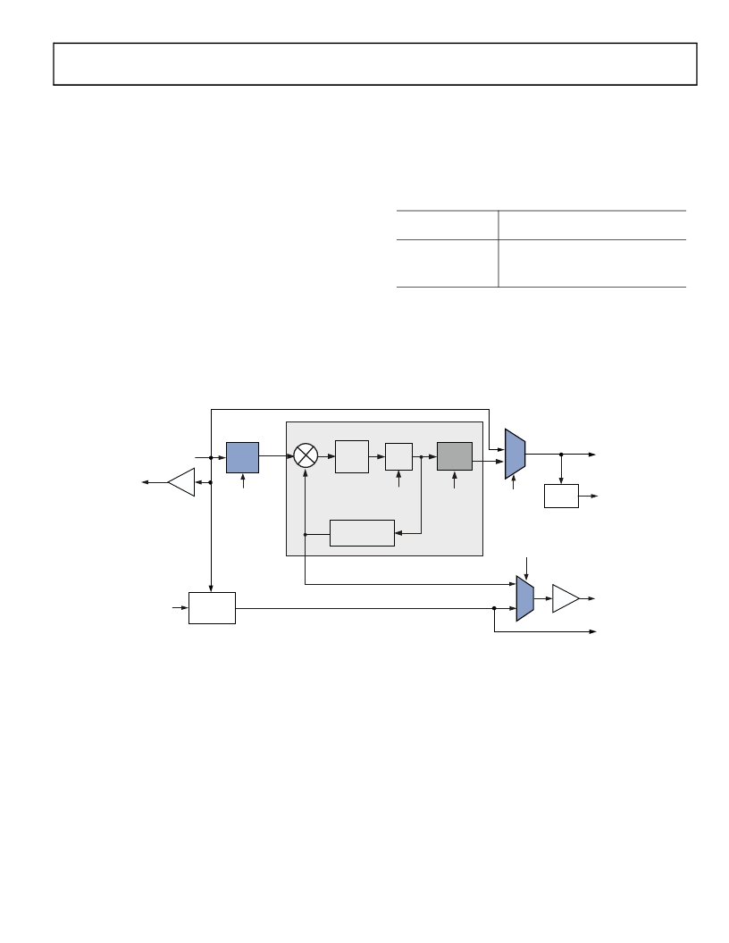
PLL
lator or crystal. The shaded divider/multiplier blocks denote
where clock ratios can be set through hardware or software
using the power management control register (PMCTL). For
more information, refer to the ADSP-2136x SHARC Processor
Hardware Reference .
CLKIN
CLKIN
DIVIDER
f INPUT
LOOP
FILTER
VCO
f VCO
PLL
DIVIDER
f CCLK
CCLK
XTAL
BUF
PMCTL
(INDIV)
CLK_CFGx/
PMCTL (2 × PLLM)
PMCTL
(2 × PLLN)
PMCTL
(PLLBP)
DIVIDE
BY 2
PCLK
f VCO ÷ (2 × PLLM)
PMCTL (CLKOUTEN)
CLKOUT (TEST ONLY)*
RESETOUT
RESET
DELAY OF
4096 CLKIN
RESETOUT
BUF
CYCLES
CORERST
*CLKOUT (TEST ONLY) FREQUENCY IS THE SAME AS f INPUT.
THIS SIGNAL IS NOT SPECIFIED OR SUPPORTED FOR ANY DESIGN.
Figure 5. Core Clock and System Clock Relationship to CLKIN
Rev. J |
Page 17 of 60 |
July 2013
发布紧急采购,3分钟左右您将得到回复。
相关PDF资料
ADZS-21371-EZLITE
KIT EVAL EZLITE ADZS-21371
ADZS-21469-EZLITE
KIT EVAL EZ LITE ADSP-21469
ADZS-21479-EZLITE
KIT EVAL EZ BOARD ADSP-2147X
ADZS-21489-EZLITE
KIT EVAL EZ BOARD ADSP-2148X
ADZS-218X-ICE-2.5V
EMULATOR SRL FOR ADDS-218X-ICE
ADZS-BF506F-EZLITE
KIT EVAL EZLITE ADSP-BF506F
ADZS-BF518F-EZLITE
KIT EZ LITE BF512F/14F/16F/18F
ADZS-BF527-EZLITE
BOARD EVAL ADSP-BF527
相关代理商/技术参数
ADZS-21369-EZLITE
功能描述:KIT EVAL EZ LITE ADDS-21369 RoHS:是 类别:编程器,开发系统 >> 通用嵌入式开发板和套件(MCU、DSP、FPGA、CPLD等) 系列:SHARC® 产品培训模块:Blackfin® Processor Core Architecture Overview
Blackfin® Device Drivers
Blackfin® Optimizations for Performance and Power Consumption
Blackfin® System Services 特色产品:Blackfin? BF50x Series Processors 标准包装:1 系列:Blackfin® 类型:DSP 适用于相关产品:ADSP-BF548 所含物品:板,软件,4x4 键盘,光学拨轮,QVGA 触摸屏 LCD 和 40G 硬盘 配用:ADZS-BFBLUET-EZEXT-ND - EZ-EXTENDER DAUGHTERBOARDADZS-BFLLCD-EZEXT-ND - BOARD EXT LANDSCAP LCD INTERFACE 相关产品:ADSP-BF542BBCZ-4A-ND - IC DSP 16BIT 400MHZ 400CSBGAADSP-BF544MBBCZ-5M-ND - IC DSP 16BIT 533MHZ MDDR 400CBGAADSP-BF542MBBCZ-5M-ND - IC DSP 16BIT 533MHZ MDDR 400CBGAADSP-BF542KBCZ-6A-ND - IC DSP 16BIT 600MHZ 400CSBGAADSP-BF547MBBCZ-5M-ND - IC DSP 16BIT 533MHZ MDDR 400CBGAADSP-BF548BBCZ-5A-ND - IC DSP 16BIT 533MHZ 400CSBGAADSP-BF547BBCZ-5A-ND - IC DSP 16BIT 533MHZ 400CSBGAADSP-BF544BBCZ-5A-ND - IC DSP 16BIT 533MHZ 400CSBGAADSP-BF542BBCZ-5A-ND - IC DSP 16BIT 533MHZ 400CSBGA
ADZS-21369-EZLITE
制造商:Analog Devices 功能描述:ADZS-21369-EZLITE
ADZS-21371-EZLITE
功能描述:KIT EVAL EZLITE ADZS-21371 RoHS:是 类别:编程器,开发系统 >> 通用嵌入式开发板和套件(MCU、DSP、FPGA、CPLD等) 系列:SHARC® 产品培训模块:Blackfin® Processor Core Architecture Overview
Blackfin® Device Drivers
Blackfin® Optimizations for Performance and Power Consumption
Blackfin® System Services 特色产品:Blackfin? BF50x Series Processors 标准包装:1 系列:Blackfin® 类型:DSP 适用于相关产品:ADSP-BF548 所含物品:板,软件,4x4 键盘,光学拨轮,QVGA 触摸屏 LCD 和 40G 硬盘 配用:ADZS-BFBLUET-EZEXT-ND - EZ-EXTENDER DAUGHTERBOARDADZS-BFLLCD-EZEXT-ND - BOARD EXT LANDSCAP LCD INTERFACE 相关产品:ADSP-BF542BBCZ-4A-ND - IC DSP 16BIT 400MHZ 400CSBGAADSP-BF544MBBCZ-5M-ND - IC DSP 16BIT 533MHZ MDDR 400CBGAADSP-BF542MBBCZ-5M-ND - IC DSP 16BIT 533MHZ MDDR 400CBGAADSP-BF542KBCZ-6A-ND - IC DSP 16BIT 600MHZ 400CSBGAADSP-BF547MBBCZ-5M-ND - IC DSP 16BIT 533MHZ MDDR 400CBGAADSP-BF548BBCZ-5A-ND - IC DSP 16BIT 533MHZ 400CSBGAADSP-BF547BBCZ-5A-ND - IC DSP 16BIT 533MHZ 400CSBGAADSP-BF544BBCZ-5A-ND - IC DSP 16BIT 533MHZ 400CSBGAADSP-BF542BBCZ-5A-ND - IC DSP 16BIT 533MHZ 400CSBGA
ADZS-21371-EZLITE
制造商:Analog Devices 功能描述:ADZS-21371-EZLITE
ADZS-21375-EZLITE
功能描述:KIT BOARD FOR EZ-LITE ADSP-217X RoHS:是 类别:编程器,开发系统 >> 通用嵌入式开发板和套件(MCU、DSP、FPGA、CPLD等) 系列:SHARC® 标准包装:1 系列:PICDEM™ 类型:MCU 适用于相关产品:PIC10F206,PIC16F690,PIC16F819 所含物品:板,线缆,元件,CD,PICkit 编程器 产品目录页面:659 (CN2011-ZH PDF)
ADZS-21469-EZBRD
功能描述:KIT EVAL EZ BOARD ADSP-21469 RoHS:是 类别:编程器,开发系统 >> 通用嵌入式开发板和套件(MCU、DSP、FPGA、CPLD等) 系列:SHARC® 产品培训模块:Blackfin® Processor Core Architecture Overview
Blackfin® Device Drivers
Blackfin® Optimizations for Performance and Power Consumption
Blackfin® System Services 特色产品:Blackfin? BF50x Series Processors 标准包装:1 系列:Blackfin® 类型:DSP 适用于相关产品:ADSP-BF548 所含物品:板,软件,4x4 键盘,光学拨轮,QVGA 触摸屏 LCD 和 40G 硬盘 配用:ADZS-BFBLUET-EZEXT-ND - EZ-EXTENDER DAUGHTERBOARDADZS-BFLLCD-EZEXT-ND - BOARD EXT LANDSCAP LCD INTERFACE 相关产品:ADSP-BF542BBCZ-4A-ND - IC DSP 16BIT 400MHZ 400CSBGAADSP-BF544MBBCZ-5M-ND - IC DSP 16BIT 533MHZ MDDR 400CBGAADSP-BF542MBBCZ-5M-ND - IC DSP 16BIT 533MHZ MDDR 400CBGAADSP-BF542KBCZ-6A-ND - IC DSP 16BIT 600MHZ 400CSBGAADSP-BF547MBBCZ-5M-ND - IC DSP 16BIT 533MHZ MDDR 400CBGAADSP-BF548BBCZ-5A-ND - IC DSP 16BIT 533MHZ 400CSBGAADSP-BF547BBCZ-5A-ND - IC DSP 16BIT 533MHZ 400CSBGAADSP-BF544BBCZ-5A-ND - IC DSP 16BIT 533MHZ 400CSBGAADSP-BF542BBCZ-5A-ND - IC DSP 16BIT 533MHZ 400CSBGA
ADZS-21469-EZLITE
功能描述:KIT EVAL EZ LITE ADSP-21469 RoHS:是 类别:编程器,开发系统 >> 通用嵌入式开发板和套件(MCU、DSP、FPGA、CPLD等) 系列:SHARC® 产品培训模块:Blackfin® Processor Core Architecture Overview
Blackfin® Device Drivers
Blackfin® Optimizations for Performance and Power Consumption
Blackfin® System Services 特色产品:Blackfin? BF50x Series Processors 标准包装:1 系列:Blackfin® 类型:DSP 适用于相关产品:ADSP-BF548 所含物品:板,软件,4x4 键盘,光学拨轮,QVGA 触摸屏 LCD 和 40G 硬盘 配用:ADZS-BFBLUET-EZEXT-ND - EZ-EXTENDER DAUGHTERBOARDADZS-BFLLCD-EZEXT-ND - BOARD EXT LANDSCAP LCD INTERFACE 相关产品:ADSP-BF542BBCZ-4A-ND - IC DSP 16BIT 400MHZ 400CSBGAADSP-BF544MBBCZ-5M-ND - IC DSP 16BIT 533MHZ MDDR 400CBGAADSP-BF542MBBCZ-5M-ND - IC DSP 16BIT 533MHZ MDDR 400CBGAADSP-BF542KBCZ-6A-ND - IC DSP 16BIT 600MHZ 400CSBGAADSP-BF547MBBCZ-5M-ND - IC DSP 16BIT 533MHZ MDDR 400CBGAADSP-BF548BBCZ-5A-ND - IC DSP 16BIT 533MHZ 400CSBGAADSP-BF547BBCZ-5A-ND - IC DSP 16BIT 533MHZ 400CSBGAADSP-BF544BBCZ-5A-ND - IC DSP 16BIT 533MHZ 400CSBGAADSP-BF542BBCZ-5A-ND - IC DSP 16BIT 533MHZ 400CSBGA
ADZS-21479-EZBRD
功能描述:BOARD EVAL FOR ADZS-2147X RoHS:是 类别:编程器,开发系统 >> 通用嵌入式开发板和套件(MCU、DSP、FPGA、CPLD等) 系列:SHARC® 标准包装:1 系列:PICDEM™ 类型:MCU 适用于相关产品:PIC10F206,PIC16F690,PIC16F819 所含物品:板,线缆,元件,CD,PICkit 编程器 产品目录页面:659 (CN2011-ZH PDF)
